本文共 57700 字,大约阅读时间需要 192 分钟。

E-EDID™ Standard
VESA
Video Electronics Standards Association
920 Hillview Court, Suite 140 Phone:(408)957-9270
Milpitas, CA 95035 Fax: (408)957-9277
|
VESA ENHANCED EXTENDED DISPLAY IDENTIFICATION DATA STANDARD
Release A, Revision 1 February 9,2000 Purpose This standard defines data formats to carry configuration information, allowing optimum use of displays.
Summary This document describes the basic 128-byte data structure “EDID 1.3”, as well as the overall layout of the data blocks that make up Enhanced EDID. The EDID 1.3 data structure is intended to be backward compatible with EDID data structures 1.0, 1.1 and 1.2 as implemented in all commercially available monitors. EDID data structure 1.3 contains enhancements to enable the Dual GTF curve concept. Use of EDID extensions described in this document assumes that the addressing method described in the Enhanced DDC standard is used.
Note This issue of the EDID document contains specifications for the mandatory core elements of Enhanced EDID. Optional EDID extensions are defined in separate documents.
|
Intellectual Propery
Copyright © 1994 – 2000 Video Electronics Standards Association. All rights reserved.
While every precaution has been taken in the preparation of this standard, the Video Electronics Standards Association and its contributors assume no responsibility for errors or omissions, and make no warranties, expressed or implied, of functionality or suitability for any purpose.
Trademarks
All trademarks used within this document are the property of their respective owners. VESA, DDC, DPMS, EDID, EVC, P&D and VDIF are trademarks of the Video Electronics Standard Association.
I2C is a trademark owned by Philips.
Patents
VESA proposals and standards are adopted by the Video Electronics Standards Association without regard as to whether their adoption may involve any patents or articles, materials, or processes. Such adoption does not assume any liability to any patent owner, nor does it assume any obligation whatsoever to parties adopting the proposals or standards documents.
Support for this Standard
Clarifications and application notes to support this standard may be written. To obtain the latest standard and any support documnetation, contact VESA.
If you have a product, which incorporates EDID, you should ask the company that manufactured your product for assistance. If you are a manufacturer, VESA can assist you with any clarification you may require. All comments or reported errors should be submitted in writing to VESA using one of the following methods.
- Fax: 408-957 9270, direct this note to Technical Support at VESA
- e-mail:
- mail: Technical Support
Video Electronics Standards Association
920 Hillview Court, Suite 140
Milpitas, CA 95035
Release A September 2, 1999
Intial release of the standard. The body of the standard is derived from the Extended Display Identification Standard Version 3.0
Release A Revision 1 February 9, 2000
Consolidate requirements of detailed timing section in section 3.10
Section 3.4 - removed restriction of 00h, 00h, 00h, 00h value for serial number field
Table 3.11 - added note to reference preferred timing mode bit requirements
Table 3.15 - added not for 1:1 aspect ratio in earlier EDID definitions
Table 3.16 - corrected order of bits in Vertical Sync format description
Table 3.17 - added definition for stereo flag bits values of 0,0,x
Table 3.10 - added clarification to round up Max pixel; clock value
Acknowledgments
This document would not have been possible without the efforts of the VESA Display Committee. In particular, the following individuals and their companies contributed significant time and knowledge to this edition, and/or previous editions of the EDID document.
Anders Frisk Nokia Jack Hosek NEC
Bob Myers HP Richard Atanus NEC
Don Panell Joe Goodart Dell
Hans van der Ven Panasonic Bill Milford 3dfx
Geoff Gould Intel Ian Miller IBM
Rick Stoneking Microchip Shaun Kerigan IBM
Glenn Adler Philips Ed Anwyl IBM
Chuck Scott Microsoft Anthony Cianfarano Mitsubishi
Alain d’Hautecourt Viewsonic Ton Wang Hitachi
Warren Whaley Canon John Matsumoto Toshiba
Drew Loucks Elo Touchsystems
The Extended Display Identificaiton Data (EDID) described in this document, is a data structure, with optional variants, to allow the display to inform the host about its identity and capabilities. The EDID data structure is independent of the communication protocol uesd between the monitor and host.
Enhanced EDID defines a basic data structure of 128 bytes that all compliant monitors must supply, as well as the rules for how extensions can be added to the basic structure.
Enhanced EDID family of document:
- Enhanced EDID Standard (Basic 28-byte data structure. Rules for how EDID extensions are mapped.)
- Optional EDID Extension Standards (Data structure for additonal data contained in EDID extensions.)
- EDID Structure 2 Extension
- Flat Panel Timings Extension
- Color transfer fucntion Extension
- …future extension structures not yet defined
Enhanced EDID was created to clarify how EDID Extensions shall be used in order to handle identification of future monitor capabilities, while maintaining a basic level of compatibility that can be used to uniquely identify the monitor. Enhanced EDID is intended to supersed all previous versions of EDID.
The EDID Standard was developed by VESA to meet, exceed and/or complement certain criteria. These criteria are set forth as Standard Objectives as follows:
- Support Microsoft® Plug and Play definition
- Provide information in a compact format to allow the graphics subsystem to be configured based on the capabilities of the attached display
Note: Versions identified here are current, but users of this standard are advised to ensure they have the latest versions of referenced standards and doctiments.
- VESA Enhanced Display Data Channel Standard - E-DDC, Verison 1, September 2, 1999
- VESA Plug & Display Standard - P&D, Version 1, June 11, 1997
- VESA Video BIOS Extensions for Display Data Channel Standard - VBE/DDC, Version 1.1, Nov. 18, 1999
- VESA Video Image Area Definition Standard - VIAD, Revision 1.0, August 12, 1993
- VESA Generalized Timing Formula Standard - GTF, Version 1.0, December 18, 1996
- Microsoft/Intel Plug and Play ISA Specification, Verison 1.0, May 28, 1993.
- Microsoft/Intel Plug and Play Errata and Clarification Document, December 10 ,1993.
- IBM Personal System/2 Hardware Interface Technical Reference - Common Interfaces Video Subsystem
EDID structure 1.0 was the original 128-byte data format introduced in the DDC Standard Version 1.0 Revison 0 issued in August 1994. EDID 1.0 shall not be used in new monitor designs released after January 1, 2000.
EDID structure 1.1 added definitions for monitor descriptors as an alternate use of the space originally reserved for detailed timings, as well as definitions for perviously unused fields. Structure 1.1 was introduced in the EDID Standard Version 2 Revision 0 issued in April 1996. EDID 1.1 shall not be used in new monitor designs released after January 1, 2000.
EDID structure 1.2 added definitions to existing data fields. Structure 1.2 was introduced in EDID Standard Version 3. EDID 1.2 is not recommended in new monitor designs released after January 1, 2000.
EDID structure 1.3 is introduced for the first time in this document and adds definitions for secondary GTF curve coefficients. EDID 1.3 is based on the same core as all other EDID 1.x structures. EDID 1.3 is intended to be the new baseline for EDID data structures. EDID 1.3 is recommended for all new monitor designs.
Structure 1.3 is a super set of structure 1.2. The main difference between the two is that 1.3 allows the Monitor Range Limits descriptor to define coefficients for a secondary GTF curve, and mandates a certain set of monitor descriptors.
Version 2 Revision 0 data structure defined a completely new EDID data structure based on 256-byte records. This structure was designed to provide additional information that is required for displays that follow the original VESA Plug & Display (P&D) and Flat Panel Display Interface-2 (FPDI-2) Standards.
NOTE! In the future, EDID structure 2.0 will be treated as an allowed, but not mandatory, EDID extension under Enhanced EDID.
E-EDID is based on EDID structure 1.3 and allows additional data stored as EDID Extensions. In the minimum configuration, E-EDID consists of one data structure—EDID structure 1.3
Compatibility with monitors and systems that require EDID structure 2 is achieved by allowing EDID structure 2 to be included in E-EDID as two extensions residing at fixed locations.
-
-
-
- Mandatory elements
-
-
Block 0 is the only mandatory block.
This table shows the required use of E-EDID blocks.
All blocks are 128 bytes in length.
Each extension block is structured according to Section 2.2.1.3.
All extension blocks must be sequential, no holes allowed
| Block# | Blcok Description |
| 0 | EDID 1.3 (or higher) |
| 1 | Extension if only 1 extension, otherwise EDID Block map (blocks 2-127) |
| 2 | Extension |
| 3 | Extension |
| 4 | Extension |
| : |
|
| N | Extension |
| : |
|
| 128 | EDID Block map for blocks 129 - 254 if more than 128 blocks used |
| 129 | Extension |
| : |
|
| N =< 254 | Extension |
|
|
|
Block number 1 is used for Extension data if there is only one extension, otherwise block 1 is used as a block map.
-
-
-
- EDID Block Map Extension
-
-
| Byte# | Description |
|
| 0 | Tag for Block Map |
|
| 1 | Extension Tag for data in block 2 or block 129 | Unused blocks are listed as Extension Tag = 0 |
| 2 | Extension Tag for data in block 3 or block 130 |
|
|
|
|
|
| N | Extension Tag for data in block N+1 or block N+128 |
|
|
|
|
|
| 126 | Extension Tag for data in block 127 or block 254 |
|
| 127 | Check sum for this block map |
|
Block Tag is a byte that identifies the content of the Extension Block. A partial list of defined Tags is listed in Section 2.2.1.4
-
-
-
- General Extension Format
-
-
| Byte # | Description |
|
| 0 | Extension tag |
|
| 1 | Revision number for this tag | One byte binary number. Revisions are backward compatible. |
| 2-126 | Extension data |
|
| 127 | Checksum for this Extension Block |
|
-
-
-
- EDID Extension Tags Assigned by VESA
-
-
VESA will maintain a list of assigned EDID Extension Tags used to identify VESA Standard EDID Extensions. For the most current list of EDID Extensions, see the VESA website.
| Tag | Description |
| 01h | LCD Timings |
| 12h | Additional timing data type 2 |
|
|
|
| 20h | EDID 2.0 Extension |
|
|
|
| 30h | Color information type 0 |
|
|
|
| 40h | DVI feature data |
|
|
|
| 50h | Touch screen data |
|
|
|
| F0h | Block map |
|
|
|
| FFh | Extension defined by monitor manufacturer |
Note: At the time of the publication of this document, several of these extensions were not yet been defined or written. Contact VESA administration for the latest list of published EDID Extensions.
- (EDID) Structure Ver. 1 Rev.
| Address | No. bytes |
| Decription | Format |
| 00h | 8 | Bytes | Header | See Section 3.3 |
| 00h |
| 1 | 00h |
|
| 01h |
| 1 | FFh |
|
| 02h |
| 1 | FFh |
|
| 03h |
| 1 | FFh |
|
| 04h |
| 1 | FFh |
|
| 05h |
| 1 | FFh |
|
| 06h |
| 1 | FFh |
|
| 07h |
| 1 | 00h |
|
| 08h | 10 | Bytes | Vendor / Product Indentificaiton | See Section 3.4 |
| 08 |
| 2 | ID Manufacturer Name | EISA 3-character ID |
| 0A |
| 2 | ID Product Code | Vender assigned code |
| 0C |
| 4 | ID Serial Number | 32-bit serial number |
| 10 |
| 1 | Week of Manufacture | Week number |
| 11 |
| 1 | Year of Manufacture | Year |
| 12h | 2 | Bytes | EDID Structure Version / Revision | See Section 3.5 |
| 12 |
| 1 | Version # | Binary |
| 13 |
| 1 | Revision # | Binary |
| 14h | 5 | Bytes | Basic Display Parameters / Features | See Section3.6 |
| 14 |
| 1 | Video Input Definition |
|
| 15 |
| 1 | Max. Horizontal Image Size | cm. |
| 16 |
| 1 | Max. Vertical Image Size | cm. |
| 17 |
| 1 | Display Transfer Characteristic (Gamma) | Binary |
| 18 |
| 1 | Feature Support | See Table 3.11 |
| 19h | 10 | Bytes | Color Characteristics | See Section 3.7 |
| 19 |
| 1 | Red/Green Low Bits | Rx1 Rx0 Ry1 Ry0 Gx1 Gx0 Gy1 Gy0 |
| 1A |
| 1 | Blue/White Low Bits | Bx1 Bx0 By1 By0 Wx1 Wx0 Wy1 Wy0 |
| 1B |
| 1 | Red-x | Red-x Bits 9 - 2 |
| 1C |
| 1 | Red-y | Red-y Bits 9 - 2 |
| 1D |
| 1 | Green-x | Grenn-x Bits 9 - 2 |
| 1E |
| 1 | Green-y | Green-y Bits 9 - 2 |
| 1F |
| 1 | Blue-x | Blue-x Bits 9 - 2 |
| 20 |
| 1 | Blue-y | Blue-y Bits 9 - 2 |
| 21 |
| 1 | White-x | White-x Bits 9 - 2 |
| 22 |
| 1 | White-y | White-y Bits 9 - 2 |
| 23h | 3 | Bytes | Established Timings | See Section 3.8 |
| 23 |
| 1 | Established Timings 1 |
|
| 24 |
| 1 | Established Timings 2 |
|
| 25 |
| 1 | Manufacturer’s Reserved Timings |
|
| 26 | 16 | Bytes | Standard Timing Identification | See Section 3.9 |
| 26 |
| 2 | Standard Timing Indentification # 1 |
|
| 28 |
| 2 | Standard Timing Indentification # 2 |
|
| 2A |
| 2 | Standard Timing Indentification # 3 |
|
| 2C |
| 2 | Standard Timing Indentification # 4 |
|
| 2E |
| 2 | Standard Timing Indentification # 5 |
|
| 30 |
| 2 | Standard Timing Indentification # 6 |
|
| 32 |
| 2 | Standard Timing Indentification # 7 |
|
| 34 |
| 2 | Standard Timing Indentification # 8 |
|
| 36h | 72 | Bytes | Detailed Timing Descriptions | See Section 3.10 |
| 36h |
| 1 | Detailed Timing Description # 1 | EDID structure Version 1, Revisions 1 and 2, allowed this space to be used for Monitor Descriptors. Host SW using this data should be prepared to detect Monitor Descriptors also in this location even though displays conforming with later revisions of EDID structure only use this space for Detailed Timing Description.
|
| 48h |
| 1 | Detailed Timing Description # 2 or Monitor Descriptor |
|
| 5Ah |
| 1 | Detailed Timing Description # 3 or Monitor Descriptor |
|
| 6Ch |
| 1 | Detailed Timing Description # 4 or Monitor Descriptor |
|
| 7Eh | 1 | Bytes | Extension Flag | Number of (optional) 128-byte EDID extension blocks to follow |
| 7Fh | 1 | Bytes | Checksum | The 1-byte sum of all 128 bytes in this EDID block shall equal zero |
Table 3.1 - EDID Structure Version 1
The following sections provide details on each byte of the EDID Version 1 data structure.
The EDID data structures are designed to be compact in their representation of data in order to fit the most information into a limited apce. To accommodate this, many data lengths have been used according to the needs of the particular data. These include fields from a single bit up to two bytes in length. In all cases, except where explicitly stated, the following conventions are used:
| Data length | Convention used | Example |
| 1 to 70 bits | Stored in order stated |
|
| 8 bits (1 byte) | Stored at location stated |
|
| 9 to 15 bits | Location of bits stated in field definition |
|
| 16 bits (2 bytes) | Bytes are a binary format (not BCD) stored in locations specified with least significant byte (LSB) stored in first location. | 1280 decimal = 0500h Stored 00 at first location 50 next location |
| Character string (More than 2 bytes) | Bytes ars ASCII, stored in order they appear in the string | “ACED” Stored 41h at first location, 43h at the next location, 45h at the next location and 44h at the next location |
Table 3.2 - Data Format Conventions
The header is an 8-byte pattern designed to be easily recognizable from other bytes in the data structure. Its format is shown in Table 3.3.
| 8 | Bytes | Header |
|
| 1 | 00h |
| 1 | FFh | |
| 1 | FFh | |
| 1 | FFh | |
| 1 | FFh | |
| 1 | FFh | |
| 1 | FFh | |
| 1 | 00h |
Table 3.3 – EDID Header
The Vendor/Product ID block is made up of several fields used to uniquely identify the monitor. The size and order of the fields is shown in the table below.
| 10 | Bytes | Vendor / Product Identification |
|
| 2 | ID Manfacturer Name |
| 2 | ID Product Code | |
| 4 | ID Serial Number | |
| 1 | Week of Manufacture | |
| 1 | Year of Manufacture |
Table 3.4 – Vendor/Product ID
The ID Manufacturer Name field, shown in Table 3.5, contains a 2-byte representation of the monitor’s manufacturer. This is the same as the EISA ID. It is based on compressed ASCII, “00001=A“…“11010=Z”.
EISA manufacturer IDs are issued by Microsoft. Contact by:
E-mail:
Fax: 425-936-7329, Attention PNPID in Building 27.
| Desciption | Byte | Bit | |||||||
| 7 | 6 | 5 | 4 | 3 | 2 | 1 | 0 | ||
| ID Manufacturer Name | 1 | 0) | (4 | 3 | 2 | 1 | 0) | (4 | 3 |
| * | Character 1 | Char 2 | |||||||
| 2 | 2 | 1 | 0) | (4 | 3 | 2 | 1 | 0) | |
| Character 2 | Character 3 | ||||||||
Table 3.5 - ID Manufacturer Name
The ID Product code field contains a 2-byte vendor assigned product code. This is used to differentiate between different models from the same manufacturer. If this field is used to represent a model number, then the number is stored in hex with the least significant byte first.
The ID serial number is a 32-bit serial number used to fifferentiate between individual instances of the same model of monitor. Its use is optional. When used, the bit order for this field follows that shown in Table 3.6. The EDID structure Version 1 Revision 1 and later offer a way to represent the serial number of the monitor as an ASCII string in a separate descriptor block.
| Description | Byte | Bit 7 | Bit 6 | Bit 5 | Bit 4 | Bit 3 | Bit 2 | Bit 1 | Bit 0 |
| ID Serial Number | 1 | (7 | 6 | 5 | 4 | 3 | 2 | 1 | 0) |
| 2 | (15 | 14 | 13 | 12 | 11 | 10 | 9 | 8) | |
| 3 | (23 | 22 | 21 | 20 | 19 | 18 | 17 | 16) | |
| 4 | (31 | 30 | 29 | 28 | 27 | 26 | 25 | 24) |
Table 3.6 - ID Serial Number
The Week of Manufacture field, if used, is set to a value in the range of 1-53. If this field is not used,the value should be set to 0.
The Year of Manufacture field is used to represent the year of the monitor’s manufacture. The value that is stored is an offset from the year 1990 as derived from the following equation:
Value stored = (Year of manufacture - 1990)
Example: For a monitor manufactured in 1997 the value stored in this field would be 7.
| 2 | Bytes | EDID Structure Version, Revision |
|
|
| 1 | Version no. | Binary |
| 1 | Revision no. | Binary |
Table 3.7 - EDID Structure Version and Revision
The appropriate verison and revision numbers shall be stored here. These values define the EDID structure being used. Products compliant with this document shall have Version = 1 and Revision = 3.
| 5 | Bytes | Basic Display Parameters/Features |
|
|
| 1 | Video Input Definition | See Table 3.9 |
| 1 | Max. Horizontal Image Size | cm. | |
| 1 | Max. Vertical Image Size | cm. | |
| 1 | Display Transfer Characteristic (Gamma) | (gamma x 100)-100, [range 1.00 → 3.54] If set to FFh, the gamma value is not defined here. | |
| 1 | Feature Support (DPMS) | See Table 3.11 |
Table 3.8 - Basic Display Parameters and Features
The Video Input Definition field provides information describing how the host’s video outputs should be configured to drive the attached display. The format of this one-byte field is described below in Table 3.9
| Bit | Description | Detailed Description |
| 7 | Analog/Digital Signal Level | Defines usage of the rest of byte as “analog” or “digital” input. Analog = 0, Digital = 1. |
|
If bit 7 = 0 use the following definitions for bit 6-0
| ||
| 6 | Signal Level Standard [6:5] | Refer to following definitions. Format is ‘reference white above blank’, ‘level of sync. tip below blank’. (volts) Bit 6 Bit 5 Operation 0 0 0.700, 0.300 (1.000 V p-p) 0 1 0.714, 0.286 (1.000 V p-p) 1 1 1.000, 0.400 (1.400 V p-p) 1 1 0.700, 0.000 (0.700 V p-p) See EVC Std. |
| 5 | Signal Level Standard [6:5] | See above entry for definition |
| 4 | Setup | If set = 1, the display expects a blank-to-black setup or pedestal per appropriate Signal Level Standard |
| 3 | Sync. Inputs Supported [3] | If set = 1, separate syncs. Supported |
| 2 | Sync. Inputs Supported [2] | If set = 1, composite sync. (on Hsync line) supported |
| 1 | Sync. Inputs Supported [1] | If set = 1, sync. on green video supported |
| 0 | Sync. Inputs Supported [0] | If set = 1, serration of the Vsync. Pulse is required when composite sync. or sync-on-green video is used |
|
If bit 7 = 1 use the following definitions for bit 6-0
| ||
| 6-1 | Reserved | Set all reserved bits to 0 |
| 0 | DFP 1.x | If set = 1, Interface is signal compatible with VESA DFP 1.x TMDS CRGB, 1 pixel / clock, up to 8 bits / color MSB aligned, DE active high |
Table 3.9 - Video Input Definition
The Maximum Image Size Parameters Provide information on the maximum image dimensions that can be correctly displayed, as defined by VESA Video Image Area Definition (VIAD) Standard, rounded to the nearest centimeter (cm). These values are intended to be the maximum image size that can be properly displayed over the entire set of supported timing/format combinations. The host system is expected to use this data to get a rough idea of the image size and aspect ratio to allow properly scaled text to be selected.
If either or both bytes are set to zero, then the system shall make no assumptions regarding the display size.
e.g. A projection display may be of indeterminate size.
| 2 | Bytes | Description | Format |
|
| 1 | Max. Horizontal Image Size | From 1 → 255 cm See above for special case = 0 |
| 1 | Max. Vertical Image Size | From 1 → 255 cm See above for special case = 0 |
Table 3.10 - Maximum Image Size
The display transfer characteristic, referred to as gamma, is stored in a 1-byte field capable of representing gamma values in the range of 1.00 to 3.54. The integer value stored is determined by the formula:
Value stored = (gamma x 100 )-100
For example, a gamma value of 2.2 would be represented as 120.
The feature support field is used to indicate support for various display features. The format of this 1-byte field is shown in following table.
| 1 | Byte | Bits | Feature Support | Description |
|
| 1
| 7 | Standby | Refer to VESA DPMS Specification |
| 6 | Suspend | Refer to VESA DPMS Specification | ||
| 5 | Active Off/Very Low Power | The display consumes much less power when it receives a timing signal that is outside its declared active operating range. The display will revert to normal operation if the timing signal returns to the normal operating range. No sync. signals is one example of a timing signal outside normal operating range. No DE signal is another example. | ||
| 4-3 | Disply Type [4:3] | Bit 4 Bit 3 Interpretation 0 0 Monochrome / grayscale display 0 1 RGB color display 1 0 Non-RGB mulicolor display e.g. R/G/Y 1 1 Undefined | ||
| 2 | Standard Default Color Space, sRGB | If this bit is set to 1, the display uses the sRGB standard default color space as its primary color space. If this bit is set, the color information in section 3.7 must match the sRGB standard values. (See example in Appendix A) | ||
| 1 | Preferred Timing Mode | If this bit is set to 1, the display’s preferred timing mode is indicated in the first detailed timing block. Note: Use of preferred timing mode is required by EDID Structure Version 1 Revision 3 and higher. | ||
| 0 | Default GTF supported | If this bit is set to 1, the display supports timings based on the GTF standard using default GTF parameter values. |
Table 3.11 - Feature Support
These bytes provide colorimetry and white point information. The data is stored in the order shown in Table 3.12.
The white point value shall be the default white point (the white point set at power on or on a reset of the display to its default setting). Provision for multiple white points is made in one of the monitor descriptors - see Section 3.10.3.
| 10 | Bytes | Color Characteristic | Based on CIE publication 15.2 on colorimetry space |
|
| 1 | Red / Green Low Bits | Rx1 Rx0 Ry1 Ry0 Gx1 Gx0 Gy1 Gy0 |
| 1 | Blue / White Low Bits | Bx1 Bx0 By1 By0 Wx1 Wx0 Wy1 Wy0 | |
| 1 | Red_x | Red_x bits 9 → 2 | |
| 1 | Red_y | Red_y bits 9 → 2 | |
| 1 | Green_x | Green_x bits 9 → 2 | |
| 1 | Green_y | Green_y bits 9 → 2 | |
| 1 | Blue_x | Blue_x bits 9 → 2 | |
| 1 | Blue_y | Blue_y bits 9 → 2 | |
| 1 | White_x | White_x bits 9 → 2 | |
| 1 | White_y | White_y bits 9 → 2 |
Table 3.12 - Chromaticity and Default White Point
The chromaticity and white point values are expressed as fractional numbers, accurate to the thousandth place.
Each number is represented by a binary fraction, which is 10 bits in length. In this fraction a value of one for the bit immediately right of the decimal point (bit 9) represents 2 raised to the -1 power. A value to 1 in the right most bit (bit 0) represents a value of 2 raised to the -10 power.
[Actual Value] = [Binary Value to Decimal] / 1024 ± 0.0005
The high order bits (9 → 2) are stored as a single byte. The low order bits (1 → 0) are paired with other low order bits to form a byte. With this representation, all values should be accurate to +/- 0.0005 of the actual value. Examples are shown in Table 3.13.
| Actual Value | Binary value | Converted Back to Decimal |
| 0.610 | 1001110001 | 0.6103516 |
| 0.307 | 0100111010 | 0.3066406 |
| 0.150 | 0010011010 | 0.1503906 |
Table 3.13 - Ten bit Binary Fraction Representation
The established timing block is a field of one-bit flags, which are used to indicate support for established VESA and other common timings in a very compact form. Other standardized timings can be described in the Standard Timings block defined in Section 3.9. Any timing can be described using the Detailed Timings block defined in Section 3.10.
Bits 6 → 0 (inclusive) of byte 3 are used to define manufacturer’s proprietary timings, and may be used if a manufacturer wants to identify such timings through the use of one-bit flags. VESA taks on responsibility for coordinating or documenting the use of these bits by any manufacturer(s).
A bit set to “1” indicates support for that timing.
Indicates Factory Supported Modes of VESA Discrete Monitor Timings (DMTs that predated EDID) as well as other industry de-facto timings that predate EDID. The one-bit flags of the Established Timing block can not be used to determine maximum format support, maximum refresh support, or any other timing parameter of the display. Also, if any one-bit flag is not set in the Established Timing block, this data can not be uesd to determine if that timing is within the supported scanning frequency of the display - only that it is not a Factory Supported Mode.
Factory Supported Modes are defined as modes that are properly sized and centered as the monitor is delivered from factory.
All Factory Supported Modes are not necessarily listed in any EDID timing section.
| 3 | Bytes | Bit | Description | Source |
|
| 1 |
| Established Timing I |
|
| 7 | 720 x 400 @ 70Hz | IBM, VGA | ||
| 6 | 720 x 400 @ 88Hz | IBM, XGA2 | ||
| 5 | 640 x 480 @ 60Hz | IBM, VGA | ||
| 4 | 640 x 480 @ 67Hz | Apple, Mac II | ||
| 3 | 640 x 480 @ 72Hz | VESA | ||
| 2 | 640 x 480 @ 75Hz | VESA | ||
| 1 | 800 x 600 @ 56Hz | VESA | ||
| 0 | 800 x 600 @ 60Hz | VESA | ||
| 1 |
| Established Timing II |
| |
| 7 | 800 x 600 @ 72Hz | VESA | ||
| 6 | 800 x 600 @ 75Hz | VESA | ||
| 5 | 832 x 624 @ 75Hz | Apple, Mac II | ||
| 4 | 1024 x 768 @ 87Hz(I) | IBM | ||
| 3 | 1024 x 768 @ 60Hz | VESA | ||
| 2 | 1024 x 768 @ 70Hz | VESA | ||
| 1 | 1024 x 768 @ 75Hz | VESA | ||
| 0 | 1280 x 1024 @ 75Hz | VESA | ||
| 1 |
| Manufacturer’s Timing I |
| |
| 7 | 1152 x 870 @ 75Hz | Apple, Mac II | ||
| 6-0 | Reserved |
|
Table 3.14 - Established Timings
The next 16 bytes provide idefntification for up to eight additional timings, each identified by a unique 2-byte code derived from the mode format and refresh rate as described below. This scheme is used to identify future standard timings not included in the Established Timings section (see Section 3.8). Standard Timing identifiers that don’t correspond to a VESA Discrete Monitor Timing Mode are referring to mode calculated using the VESA GTF with default coefficients. The scheme may also be used in monitors intended to be uesd exclusively with proprietary systems where the host already has the complete timing information. Additional standard timings may be listed by using one of the alternate definitions of the detailed Timing Descriptions permitted in EDID Structure Version 1, Revision 1 and higher - see Section 3.10.3.
Note: The 2-byte identifier codes for VESA standard timing modes are defined as part of each VESA Timing Standard.
Unused fields in this section shall be set to 01h, 01h.
The Standard Timings section is used to identify Factory Supported Modes that fall into one or both of two categories:
- VESA Discrete Monitor Timings (listed in the VESA DMT Standards document) not included in the current Established Timing section.
- Discrete timing modes calculated using GTF.
A 2-byte timing identifier identifies each timing mode. If a timing identifier listed corresponds to an issued VESA Discrete Montitor Timing, factory adjustment data must be stored (preset) in the display. If a timing idenifier listed does not match a VESA DMT identifier, it shall refer to a timing calculated using the Generalized Timing Formula (GTF) .
Factory Supported Modes are defined as modes that are properly sized and centered as the monitor is delivered from factory.
All Factory Supported Modes are not necessarily listed in any EDID timing section.
| 16 | Byte | Bit | Description | Source |
| 2 |
|
| Standard Timing Identification 1 | Comment |
|
| 1 |
| (Horizontal active pixels / 8) – 31 | The range of horizontal active pixels that can be described in each byte is 256 → 2288 pixels, in increments of 8 pixels. |
|
| 1 | 7,6
5→0 | Image Aspect ratio
Bit 7 Bit 6 Operation 0 0 16:10 Aspect ratio 0 1 4:3 Aspect ratio 1 0 5:4 Aspect ratio 1 1 16:9 Aspect ratio
Refresh Rate (Hz) - 60 | The vertical active line count may be calculated from the aspect ratio and the Horizontal active pixel count given in the first byte. “Square” pixels (1:1 pixel aspect ratio) shall be assumed. Note: EDID structures prior to Version 1 Revision 3 defined the bit combination of 0 0 to indicate a 1:0 aspect ratio
Range 60 → 123Hz |
| 2 |
|
| Standard Timing Identification 2 | See above definition for Standard Timing 1 |
| 2 |
|
| Standard Timing Identification 3 | See above definition for Standard Timing 1 |
| 2 |
|
| Standard Timing Identification 4 | See above definition for Standard Timing 1 |
| 2 |
|
| Standard Timing Identification 5 | See above definition for Standard Timing 1 |
| 2 |
|
| Standard Timing Identification 6 | See above definition for Standard Timing 1 |
| 2 |
|
| Standard Timing Identification 7 | See above definition for Standard Timing 1 |
| 2 |
|
| Standard Timing Identification 8 | See above definition for Standard Timing 1 |
Table 3.15 – Standard Timings
The detailed timing section is divided into four descriptor blocks, which are 18 bytes each. These descriptor blocks contain either timing data as described in section 3.10.2 or other types of data as described in section 3.10.3. Use of the detailed timing section shall meet the following requirements.
- All blocks shall filled with valid data using the formats described in sections 3.10.2 and 3.10.3. Use of a data fill pattern is not permitted.
- Timing data must represent a supported mode of the display.
- Descriptor blocks shall be ordered such that all detailed timing blocks precede other types of descriptor blocks
- The first descriptor block shall be used to indicate the display’s preferred timing mode. This is described in section 3.10.1.
- A Monitor Range Limits Descriptor must be provided.
- A Monitor Name Descriptor must be provided.
Example A: Preferred Detailed Timing, Detailed Timing 2, Monitor Name, Monitor Range Limits.
Example B: Preferred Detailed Timing, Monitor Serial Number, Monitor Range Limits, Monitor Name.
Note: Items 4, 5 and 6 above were permitted but not required prior to EDID structure version 1 revision 3. Hosts may encounter displays using EDID version 1 revision 0-2 which do not meet all of these requirements.
The first Detailed Timing shall only be used to indicate the mode that the monitor vendor has determined will give an optimal image. For LCD monitors, this will in most cases be the panel “native timing” and “native resolution”. Use of the EDID Preferred Timing bit shall be used to indicate that the timing indeed conforms to this definition.
| 18 | Bytes | Detailed Timing Descriptions | Format |
|
| 2 | Pixel clock / 10,000 | Stored LSB first Example : 135MHz would be 13500 decimal, Stored as BCh, 34h |
| 1 | Horizontal Active | Pixels, lower 8 bits | |
| 1 | Horizontal Blanking | Pixels, lower 8 bits | |
| 1 | Horizontal Active : Horizontal Blanking | Upper nibble : upper 4 bits of Horizontal Active Lower nibble : upper 4 bits of Horizontal Blanking | |
| 1 | Vertical Active | Pixels, lower 8 bits | |
| 1 | Vertical Blanking | Pixels, lower 8 bits | |
| 1 | Vertical Active : Vertical Blanking | Upper nibble : upper 4 bits of Vertical Active Lower nibble : upper 4 bits of Vertical Blanking | |
| 1 | Horizontal Sync. Offset | Pixels, from blanking starts, lower 8 bits | |
| 1 | Horizontal Sync Pulse Width | Pixels, lower 8 bits | |
| 1 | Vertical Sync Offset : Vertical Sync Pulse Width | Upper nibble : lines, lower 4 bits of Vertical Sync Offset Lower nibble : lines, lower 4 bits of Vertical Sync Pulse Width | |
| 1 | Horizontal Sync Offset Horizontal Sync Pulse Width Vertical Sync Offset Vertical Sync Pulse Width | Bits 7,6 : upper 2 bits of Horizontal Sync Offset Bits 5,4 : upper 2 bits of Horizontal Sync Pulse Width Bits 3,2 : upper 2 bits of Vertical Sync Offset Bits 1,0 : upper 2 bits of Vertical Sync Pulse Width | |
| 1 | Horizontal Image Size | Mm, lower 8 bits | |
| 1 | Vertical Image Size | Mm, lower 8 bits | |
| 1 | Horizontal & Vertical Image Size | Upper nibble : upper 4 bits of Horizontal Image Size Lower nibble : upper 4 bits of Vertical Image Size | |
| 1 | Horizontal Border | Pixels, see Section 3.12 | |
| 1 | Vertical Border | Lines, see Section 3.12 | |
| 1 | Flags | Interlace, Stereo, Horizontal polarity, Vertical polarity, Sync Configuration, etc. Bit 7 Function 0 Non-interlaced 0 Interlaced
Bit 6 Bit 5 Function 0 0 Normal display, no stereo x x See Table 3.17 for definition
Bit 4 Bit 3 Function 0 0 Analog composite 0 1 Bipolar analog composite 1 0 Digital composite 1 1 Digital separate
Bit 2 Bit 1 Function The interpretation of bits 2 and 1 is dependent on the decode of bits 4 and 3 – see Table 3.18.
Bit 0 See Table 3.17 for definition |
Table 3.16 - Detailed Timing Description
| Bit 6 | Bit 5 | Bit 0 | Definition |
| 0 | 0 | x | Normal display, no stereo. The value of bit 0 is “don’t care” |
| 0 | 1 | 0 | Field sequential stereo, right image when stereo sync. = 1 |
| 1 | 0 | 0 | Field sequential stereo, left image when stereo sync. = 1 |
| 0 | 1 | 1 | 2-way interleaved stereo, right image on even lines |
| 1 | 0 | 1 | 2-way interleaved stereo, left image on even lines |
| 1 | 1 | 0 | 4-way interleaved stereo |
| 1 | 1 | 1 | Side-by-Side interleaved stereo |
Table 3.17 - Decode of Stereo Mode Bits
The sync scheme for a detailed timing is described in bits 4-1 of the Flag byte. Bits 4 and 3 describe one of four schemes. Bits 2 and 1 give further details dependent on the values in bits 4 and 3. This is shown in Table 3.18.
| Bits 4 and 3 | Bit 2 | Bit 2 Def. | Bit 1 | Bit 1 Def. |
| 0,0 Analog Composite | Serrate | If set, controller shall supply serration (Hsync during Vsync). | On RGB | If set, sync pulses should appear on all 3 video signal lines. If not set, sync on green video line only. |
| 0,1 Bipolar Analog Composite | Serrate | If set,controller shall supply serration (Hsync during Vsync). | On RGB | If set, sync pulses should appear on all 3 video signal lines. If not set, sync on green video line only. |
| 1,0 Digital Composite | Serrate | If set, controller shall supply serration (Hsync during Vsync). | Composite Polarity | This is the polarity of the Hsync pulses outside of Vsync. Polarity is positive if bit is set to 1. |
| 1,1 Digital Separate | Vertical Polarity | Vsync signal Polarity is Positive if bit is set to 1. | Horizontal Polarity | Hsync signal polarity is Positive if bit is set to 1. |
Table 3.18 - Sync Signal Description
The last three of the 18-byte Detailed Timing Description blocks may alternately be defined as Monitor Descriptor blocks using the general format shown in Table 3.19. Detailed descriptions of the data types are shown in Table 3.20. Those 18-byte blocks not used for Monitor Descriptors shall be used for detailed timings.
Notes regarding EDID Monitor Range Limits Descriptor
Use of this descriptor is mandatory.
Any timing outside these limits may cause the monitor to enter a self-protection mode. The host shall always verify that an intended timing falls within these limits before the timing is applied.
| 18 | Bytes | Monitor Descriptor | Values |
|
| 2 | Flag | Flag = 0000h when block used as descriptor |
| 1 | Flag | Reserved = 00h when block used as descriptor | |
| 1 | Data Type Tag (Binary coded) | FFh: Monitor Serial Number – Stored as ASCII, code page # 437, ≤ 13 bytes. FEh: ASCII String – Stored as ASCII, code page # 437, ≤ 13 bytes. FDh: Monitor range limits, binary coded FCh: Monitor name, stored as ASCII, code page # 437 FBh: Descriptor contains additional color point data FAh: Descriptor contains additional Standard Timing Identifications F9h – 11h: Currently undefined 10h: Dummy descriptor, used to indicate that the descriptor space is unused 0Fh – 00h: Descriptor defined by manufacturer. | |
| 1 | Flag | 00h when block used as descriptor | |
| 13 | Descriptor Data | Definition dependent on data type tag chosen. Tag definitions in Table 3.20 |
Table 3.19 - Monitor Descriptor Block Summary
| Data Tag | Monitor Descriptor Data | Format |
| FFh | Monitor S/N (ASCII) | If < 13 bytes then terminate with ASCII code 0Ah and pad field with ASCII code 20h. Data shall be sequence such that 1st byte = 1st character etc. |
| FEh | ASCII Data String | If < 13 bytes then terminate with ASCII code 0Ah and pad field with ASCII code 20h. Data shall be sequence such that 1st byte = 1st character etc. |
| FDh | Monitor Range Limits | Byte 5: Min. Vertical rate (for interlace this refers to field rate) Binary coded rate in Hz., integer only Byte 6: Max. Vertical rate (for interlace this refers to field rate) Binary coded rate in Hz., integer only Byte 7: Min. Horizontal in kHz, integer only, binary coded Byte 8: Max. Horizontal in kHz, integer only, binary coded Byte 9: Max. Supported Pixel Clock (as defined by the display manufacturer) Binary coded clock rate in MHz / 10 e.g. 130MHz is 0Dh Note: Maximum Pixels Clock values that are not a multiple of 10MHz should be rounded up to a multiple of 10MHz e.g. 108MHz is 0Bh
Secondary timing formula support Bytes 10 - 17 are used to indicate support for a secondary timing formula.
Byte 10 00h = No secondary timing formula supported (Support for default GTF indicated in feature byte - Table 3.11) 02h = Secondary GTF curve supported All other values = Reserved for future timing formula definitions
If Byte 10 = 00h No secondary timing formula supported, the following applies: Byte 11: Set = 0Ah. Byte 12-17: Set = 20h.
If Byte 10 = 02h Secondary GTF supported, the following applies: The standard Generalized Timing Formula with modified C, M, K and J parameters is used for a secondary timing curve. For definition of these GTF parameters, see the VESA GTF standard.
Byte 11: Reserved Set = 00A Byte 12: Start frequency for secondary curve, Hor. Freq./2 [kHz] Byte 13: C*2 0=<C=<127 Byte 14 and 15: M (LSB) 0=<M=<65535 Byte 16: K 0=<K=<255 Byte 17: J*2 0=<J=<127
|
| FCh | Monitor Name (ASCII) | If < 13 bytes then terminate with ASCII code 0Ah and pad field with ASCII code 20h. Note: Intent of this field is to provide a meaningful name to the user |
| Data Tag | Monitor Descriptor Data | Format |
| FBh | Color Point | Note: Chromaticity data to be coded as Section 3.7 Note: Gamma data to be coded as Section 3.7 Byte 5 : White point index number (binary) Byte 6 : White low bits Byte 7 : White_x Byte 8 : White_y Byte 9 : White Gamma Byte 10 : White point index number (binary) Byte 11 : White low bits Byte 12 : White_x Byte 13 : White_y Byte 14 : White Gamma Byte 15 : Set = 0Ah Byte 16 - 17 : Set = 20h Note: An index number of 00h indicates that no color point data follows |
| FAh | Standard Timing Identifiers | Note: Data format as Section 3.9 Bytes 5 & 6 : Standard Timing Identification 9 Bytes 7 & 8 : Standard Timing Identification 10 Bytes 9 & 10 : Standard Timing Identification 11 Bytes 11 & 12 : Standard Timing Identification 12 Bytes 13 & 14 : Standard Timing Identification 13 Bytes 15 & 16 : Standard Timing Identification 14 Byte 17 : Set = 0Ah Note: It is permissible to redefine more than one detailed timing block as Standard Timing Identifiers. |
| 00-0Fh | Manufacturer Specified | Note: Descriptors with data type tags in this range are defined by the monitor manufcturers and are not specified by VESA. Questions regarding interpretation should be directed to the monitor manufacturer. Note: EDID structure Version 1 Revision 1 reserved only tags 00h & 01h for manufacturer specific use. |
Table 3.20 - Monitor Descriptor Details
| 2 | Bytes | Description | Function |
|
| 1 | Extension Flg | Indicates the number of (optional) Extension EDID blocks to follow. |
| 1 | Checksum | This byte should be programmed such that a one-byte checksum of the entire 128-byte EDID equals 00h. |
Table 3.21 - Extension Flag and Checksum
This section is included to provide a frame of reference for the use of borders in detailed timings.
- Both the horizontal and vertical border sizes are for one side only. (i.e. the actual number of pixels or lines taken up by both borders is twice the listed value)
- Borders are assumed to be symmetric.
- Borders are not considered part of the active image time and do not affect the total line time, which should always be found by adding the active and blanking times for each axis.
- Borders may be part of the blanking time, but that portion that may be safely used to provide an illuminated sold-color border around the active image area.
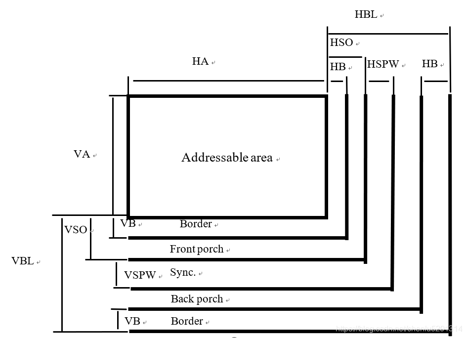
VBL Vertical Blanking HBL Horizontal Blanking
VA Vertical Active HA Horizontal Active
VB Vertical Border HB Horizontal Border
VSO Vertical Sync. Offset HSO Horizontal Sync. Offset
VSPW Vertical Sync. Pulse Width HSPW Horizontal Sync. Pulse Width
Extensions to the basic 128-byte EDID structure are defined in separate VESA Standard documents.
At the time of writing this document the following extensions are planned:
LCD Monitor Timing extension
Standard Timing extension
Color information
EDID Structure 2.0 as extension under E-EDID
The basic 128-byte EDID data structure contains four different types of timing information, Established, Standard, Preferred and Detailed timings.
The monitor should populate these data fields with the understanding that the host will evaluate and support the timing modes in the following priority order:
| PRIORITY | If GTF supported as indicated by any GTF flag in EDID | If GTF not supported |
| 1 | Preferred Detailed Timing | Preferred Detailed Timing |
| 2 | Other Detailed Timings if present | Other Detailed Timings if present |
| 3 | Standard Timings in order listed (first listed timing has highest priority) | Standard Timings in order listed (first listed timing has highest priority) |
| 4 | Any GTF timing that falls within the range limits of the monitor. All range limits parameters must be evaluated and verified to be within the limits. | Any Established Timing listed as supported |
| 5 | Any Established Timing listed as supported | Any Default GTF mode that falls within the indicate monitor range limits. Image may not be perfectly centered. |
HOSTS SHOULD NOT USE ANY OTHER TIMINGS UNLESS THEY HAVE POSITIVELY IDENTIFIED THE MONITOR AND HAVE PRIOR KNOWLEDGE ABOUT OTHER SUPPORTED MODES.
If additional timing information is contained in EDID extensions, the timing priority order should be according to the rules established in the VESA Standard describing the first listed EDID extension.
For example the LCD Timings extension may specify that the timings contained in the LCD Extension have higher priority than the timings listed in the basic EDID structure.
If there is an extension with Standard timings, the VESA Standard describing this extension may specify that the standard timings listed in the extension have priority immediately before the standard timings in the basic EDID structure. Otherwise, the priority order is the one specified in this document.
| BYTE HEX | FUNCTION | Value HEX | BIN | DEC | ASCII | Notes |
| 0 | Header | 00 | 00000000 | 0 |
|
|
| 1 |
| FF | 11111111 | 255 |
|
|
| 2 |
| FF | 11111111 | 255 |
|
|
| 3 |
| FF | 11111111 | 255 |
|
|
| 4 |
| FF | 11111111 | 255 |
|
|
| 5 |
| FF | 11111111 | 255 |
|
|
| 6 |
| FF | 11111111 | 255 |
|
|
| 7 |
| 00 | 00000000 | 0 |
|
|
| 8 | EISA Manuf. Code LSB | 10 | 00010000 | 16 |
| DELL EISA ID |
| 9 | Compressed ASCII | AC | 10101100 | 172 |
|
|
| 0A | Product code | AB | 10101011 | 171 |
| DELL Product code |
| 0B | Hex, LSB first | 50 | 01010000 | 80 |
|
|
| 0C | 32-bit ser # | 00 | 00000000 | 0 |
|
|
| 0D |
| 00 | 00000000 | 0 |
|
|
| 0E |
| 00 | 00000000 | 0 |
|
|
| 0F |
| 00 | 00000000 | 0 |
|
|
| 10 | Week of manufacture | 2A | 00101010 | 42 |
|
|
| 11 | Year of manufacture | 09 | 00001001 | 9 |
|
|
| 12 | EDID Structure Ver. | 01 | 00000001 | 1 |
|
|
| 13 | EDID revision # | 03 | 00000011 | 3 |
|
|
| 14 | Video input definition | 0E | 00001110 | 14 |
|
|
| 15 | Max H image size | 26 | 00100110 | 38 |
| 38 cm |
| 16 | Max V image size | 1D | 00011101 | 29 |
| 29 cm |
| 17 | Display Gamma | 96 | 10010110 | 150 |
| Gamma 2.5 |
| 18 | Feature support | EF | 11101111 | 239 |
| Stand-by, Suspend, Active Off RGB Color sRGB supported Preferred Timing Default GTF supported |
| 19 | Red/green low bits | EE | 11101110 | 238 |
|
|
| 1A | Blue/white low bits | 91 | 10010001 | 145 |
|
|
| 1B | Red x / high bits | A3 | 10100011 | 163 |
| Red x 0.6400 = 1010001111 |
| 1C | Red y | 54 | 01010100 | 84 |
| Red y 0.3300 = 0101010010 |
| 1D | Green x | 4C | 01001100 | 76 |
| Green x 0.3000 = 0100110011 |
| 1E | Green y | 99 | 10011001 | 153 |
| Green y 0.6000 = 1001100110 |
| 1F | Blue x | 26 | 00100110 | 38 |
| Blue x 0.1500 = 00100110010 |
| 20 | Blue y | 0F | 00001111 | 15 |
| Blue y 0.0600 = 0000111101 |
| 21 | White x | 50 | 01010000 | 80 |
| White x 0.3000 = 0101000000 |
| 22 | White y | 54 | 01010100 | 84 |
| White y 0.6000 = 0101010001 |
| 23 | Established timing I | A5 | 10100101 | 165 |
| 720x400 @70Hz 640x480 @60Hz |
| BYTE HEX | FUNCTION | Value HEX | BIN | DEC | ASCII | Notes |
|
|
|
|
|
|
| 640x480 @75Hz 800x600 @60Hz |
| 24 | Established timing II | 43 | 01000011 | 67 |
| 800x600 @75Hz 1024x768 @75Hz 1280x1024 @75Hz |
| 25 | Established timing III | 00 | 00000000 | 0 |
|
|
| 26 | Standard timing # 1 | A9 | 10101001 | 169 |
| 1600x1200 @75Hz |
| 27 |
| 4F | 01001111 | 79 |
|
|
| 28 | Standard timing # 2 | A9 | 10101001 | 169 |
| 1600x200 @85Hz |
| 29 |
| 59 | 01011001 | 89 |
|
|
| 2A | Standard timing # 3 | 71 | 01110001 | 113 |
| 1152x864 @85Hz |
| 2B |
| 59 | 01011001 | 89 |
|
|
| 2C | Standard timing # 4 | 61 | 01100001 | 97 |
| 1024x768 @85Hz |
| 2D |
| 59 | 01011001 | 89 |
|
|
| 2E | Standard timing # 5 | 45 | 01000101 | 69 |
| 800x600 @85Hz |
| 2F |
| 59 | 01011001 | 89 |
|
|
| 30 | Standard timing # 6 | 31 | 00110001 | 49 |
| 640x480 @85Hz |
| 31 |
| 59 | 01011001 | 89 |
|
|
| 32 | Standard timing # 7 | C2 | 11000010 | 194 |
| 1800x1440 @75Hz |
| 33 |
| 8F | 10001111 | 143 |
|
|
| 34 | Standard timing # 8 | 01 | 00000001 | 1 |
| NOT USED |
| 35 |
| 01 | 00000001 | 1 |
|
|
| 36 | Detailed timing /monitor descriptor # 1 | 86 | 10000110 | 134 |
|
|
| 37 | 1280x1024 @85Hz, 157.5MHz | 3D | 00111101 | 61 |
|
|
| 38 | Hor active = 1280 pixels | 00 | 00000000 | 0 |
|
|
| 39 | Hor blanking = 448 pixels | C0 | 11000000 | 192 |
|
|
| 3A |
| 51 | 01010001 | 81 |
|
|
| 3B | Vertical active = 1280 lines | 00 | 00000000 | 0 |
|
|
| 3C | Vertical blanking = 448 lines | 30 | 00110000 | 48 |
|
|
| 3D |
| 40 | 01000000 | 64 |
|
|
| 3E | Hor sync. offset = 64 pixels | 40 | 01000000 | 64 |
|
|
| 3F | H sync. width = 160 pixels | A0 | 10100000 | 160 |
|
|
| 40 | V sync. offset = 1 lines | 13 | 00010011 | 19 |
|
|
| 41 | V sync. width = 3 lines | 00 | 00000000 | 0 |
|
|
| 42 | H image size = 380 mm | 7C | 01111100 | 124 |
|
|
| 43 | V image size = 290 mm | 22 | 00100010 | 34 |
|
|
| 44 |
| 11 | 00010001 | 17 |
|
|
| 45 | No Horizontal border | 00 | 00000000 | 0 |
|
|
| 46 | No Vertical Border | 00 | 00000000 | 0 |
|
|
| 47 | Separate digital syncs., H / V polarity = +/+ | 1E | 00011110 | 30 |
|
|
| 48 | Detailed timing /monitor descriptor # 2 | 00 | 00000000 | 0 |
|
|
| 49 | Monitor serial Number | 00 | 00000000 | 0 |
|
|
| 4A | “55347BONZH47” | 00 | 00000000 | 0 |
|
|
| 4B |
| FF | 11111111 | 255 |
|
|
| 4C |
| 00 | 00000000 | 0 |
|
|
| 4D |
| 35 | 00110101 | 53 | 5 |
|
| 4E |
| 35 | 00110101 | 53 | 5 |
|
| 4F |
| 33 | 00110011 | 51 | 3 |
|
| 50 |
| 34 | 00110100 | 52 | 4 |
|
| 51 |
| 37 | 00110111 | 55 | 7 |
|
| 52 |
| 42 | 01000010 | 66 | B |
|
| BYTE HEX | FUNCTION | Value HEX | BIN | DEC | ASCII | Notes |
| 53 |
| 4F | 01001111 | 79 | O |
|
| 54 |
| 4E | 01001110 | 78 | N |
|
| 55 |
| 5A | 01011010 | 90 | Z |
|
| 56 |
| 48 | 01001000 | 72 | H |
|
| 57 |
| 34 | 00110100 | 52 | 4 |
|
| 58 |
| 37 | 00110111 | 55 | 7 |
|
| 59 |
| 0A | 00001010 | 10 |
|
|
|
|
|
|
|
|
|
|
| 5A | Detailed timing /monitor Descriptor # 3 | 00 | 00000000 | 0 |
|
|
| 5B |
| 00 | 00000000 | 0 |
|
|
| 5C | Monitor name | 00 | 00000000 | 0 |
|
|
| 5D | “DELL UR111” | FC | 11111100 | 252 |
|
|
| 5E |
| 00 | 00000000 | 0 |
|
|
| 5F |
| 44 | 01000100 | 68 | D |
|
| 60 |
| 45 | 01000101 | 69 | E |
|
| 61 |
| 4C | 01001100 | 76 | L |
|
| 62 |
| 4C | 01001100 | 76 | L |
|
| 63 |
| 20 | 00100000 | 32 |
|
|
| 64 |
| 55 | 01010101 | 85 | U |
|
| 65 |
| 52 | 01010010 | 82 | R |
|
| 66 |
| 31 | 00110001 | 49 | 1 |
|
| 67 |
| 31 | 00110001 | 49 | 1 |
|
| 68 |
| 31 | 00110001 | 49 | 1 |
|
| 69 |
| 0A | 00001010 | 10 |
|
|
|
|
|
|
|
|
|
|
| 6A |
| 20 | 00100000 | 32 |
|
|
| 6B |
| 20 | 00100000 | 32 |
|
|
| 6C | Detailed timing /monitor descriptor # 4 | 00 | 00000000 | 0 |
|
|
| 6D |
| 00 | 00000000 | 0 |
|
|
| 6E | MONITOR RANGE LIMITS | 00 | 00000000 | 0 |
|
|
| 6F |
| FD | 11111101 | 253 |
|
|
| 70 |
| 00 | 00000000 | 0 |
|
|
| 71 | Vert range | 30 | 00110000 | 48 |
| 48Hz |
| 72 |
| A0 | 10100000 | 160 |
| 160Hz |
| 73 | Horizontal range | 1E | 00011110 | 30 |
| 30kHz |
| 74 |
| 79 | 01111001 | 121 |
| 121kHz |
| 75 | Max Dot Clock | 1C | 00011100 | 28 |
| 280MHz |
| 76 | Secondary GTF | 02 | 00000010 | 2 |
|
|
| 77 | Reserved 00 | 00 | 00000000 | 0 |
|
|
| 78 | Start freq. 80kHz | 28 | 00101000 | 40 |
|
|
| 79 | C=40 | 50 | 01010000 | 80 |
|
|
| 7A | M=3600 | 10 | 00010000 | 16 |
|
|
| 7B |
| 0E | 00001110 | 14 |
|
|
| 7C | K=128 | 80 | 10000000 | 128 |
|
|
| 7D | J=35 | 46 | 01000110 | 70 |
|
|
| 7E | Extension Flag | 00 | 00000000 | 0 |
|
|
| 7F | Checksum | 8D | 10001101 | 141 |
|
|
Version 1 Revision 1 data structure format
This sample EDID is included for illustration only, it should not be considered as representative of any particular monitor. Note that this EDID Ver.1 Rev. 1 is only included as an example of legacy EDID data that a new E-EDID aware host may encounter. All new monitors shall conform to EDID structure Version 1 Rev 3.
| Byte # (decimal) | Byte # (HEX) | Field Name and Comments | Value (HEX) | Value (binary) |
| 0 | 00 | Header | 00 | 00000000 |
| 1 | 01 |
| FF | 11111111 |
| 2 | 02 |
| FF | 11111111 |
| 3 | 03 |
| FF | 11111111 |
| 4 | 04 |
| FF | 11111111 |
| 5 | 05 |
| FF | 11111111 |
| 6 | 06 |
| FF | 11111111 |
| 7 | 07 |
| 00 | 00000000 |
| 8 | 08 | EISA manufacturer code = IBM | 24 | 00100100 |
| 9 | 09 | (Compressed ASCII) | 4D | 01001101 |
| 10 | 0A | Product code = 6542 | 8E | 10001110 |
| 11 | 0B | (Hex, LSB first) | 19 | 00011001 |
| 12 | 0C | 32-bit serial number = 00000000 | 00 | 00000000 |
| 13 | 0D |
| 00 | 00000000 |
| 14 | 0E |
| 00 | 00000000 |
| 15 | 0F |
| 00 | 00000000 |
| 16 | 10 | Week of manufacture = 10 | 0A | 00001010 |
| 17 | 11 | Year of manufacture = 1995 | 05 | 00000101 |
| 18 | 12 | EDID Structure version # = 1 | 01 | 00000001 |
| 19 | 13 | EDID revision # = 1 | 01 | 00000001 |
| 20 | 14 | Video input definition = Analog i/p, 1.0 Vp-p, separate syncs | 08 | 00001000 |
| 21 | 15 | Max H image size (cm) = 40 cm | 28 | 00101000 |
| 22 | 16 | Max V image size (cm) = 30 cm | 1E | 00011110 |
| 23 | 17 | Display gamma = 2.8 | B4 | 10110100 |
| 24 | 18 | Feature support (DPMS) = Standby, Suspend, RGB Color | C8 | 11001000 |
| 25 | 19 | Red / Green low bits | 00 | 00000000 |
| 26 | 1A | Blue / White low bits | B2 | 10110010 |
| 27 | 1B | Red x Rx = 0.625 | A0 | 10100000 |
| 28 | 1C | Red y Ry = 0.340 | 57 | 01010111 |
| 29 | 1D | Green x Gx = 0.285 | 49 | 01001001 |
| 30 | 1E | Green y Gy = 0.605 | 9B | 10011011 |
| 31 | 1F | Blue x Bx = 0.150 | 26 | 00100110 |
| 32 | 20 | Blue y By = 0.065 | 10 | 00010000 |
| 33 | 21 | White x Wx = 0.281 | 48 | 01001000 |
| 34 | 22 | White y Wy = 0.311 | 4F | 01001111 |
| 35 | 23 | Established timings I = 720 x 400 @ 70Hz 640 x 480 @ 60Hz, 75Hz | A4 | 10100100 |
| 36 | 24 | Established timings II = 800 x 600 @ 72Hz, 75Hz 1024 x 768 @ 60 Hz, 70Hz, 75Hz 1280 x 1024 @ 75Hz | CF | 11001111 |
| 37 | 25 | Extablished timings III / Manufacturer’s reserved timings 640 x 480, 800 x 600, 1024 x 768, 1280 x 1024 @ 85Hz 1600 x 1280 @ 75Hz | 7C | 01111100 |
| Byte # (decimal) | Byte # (HEX) | Field Name and Comments | Value (HEX) | Value (binary) |
| 38 | 26 | Standard timing identification # 1 | 31 | 00110001 |
| 39 | 27 | 640 x 480 @ 70 Hz | 4A | 01001010 |
| 40 | 28 | Standard timing identification # 2 | A9 | 10101001 |
| 41 | 29 | 1600 x 1200 @ 60 Hz | 40 | 01000000 |
| 42 | 2A | Standard timing identification # 3 | A9 | 10101001 |
| 43 | 2B | 1600 x 1200 @ 70 Hz | 4A | 01001010 |
| 44 | 2C | Standard timing identification # 4 | A9 | 10101001 |
| 45 | 2D | 1600 x 1200 @ 75 Hz | 4F | 01001111 |
| 46 | 2E | Standard timing identification # 5 | 81 | 10000001 |
| 47 | 2F | 1280 x 1024 @ 60 Hz | 80 | 10000000 |
| 48 | 30 | Standard timing identification # 6 | 01 | 00000001 |
| 49 | 31 | Unused | 01 | 00000001 |
| 50 | 32 | Standard timing identification # 7 | 01 | 00000001 |
| 51 | 33 | Unused | 01 | 00000001 |
| 52 | 34 | Standard timing identification # 8 | 01 | 00000001 |
| 53 | 35 | Unused | 01 | 00000001 |
| 53 | 36 | Detailed timing descriptor # 1 / Monitor Descriptor # 1 | 10 | 00010000 |
| 55 | 37 | 720 x 350 @ 70Hz mode : pixel clock = 28.32 MHz | 0B | 00001011 |
| 56 | 38 | Horizontal active = 720 pixels | D0 | 11010000 |
| 57 | 39 | Horizontal blanking = 180 pixels | B4 | 10110100 |
| 58 | 3A |
| 20 | 00100000 |
| 59 | 3B | Vertical active = 350 lines | 5E | 01011110 |
| 60 | 3C | Vertical blanking = 99 lines | 63 | 01100011 |
| 61 | 3D |
| 10 | 00010000 |
| 62 | 3E | Horizontal sync. offset = 18 pixels | 12 | 00010010 |
| 63 | 3F | Horizontal sync. width = 108 pixels | 6C | 01101100 |
| 64 | 40 | Vertical sync. offset = 38 lines | 62 | 01100010 |
| 65 | 41 | Vertical sync. width = 2 lines | 08 | 00001000 |
| 66 | 42 | Horizontal image size = 250 mm | FA | 11111010 |
| 67 | 43 | Vertical image size = 184 mm | B8 | 10111000 |
| 68 | 44 |
| 00 | 00000000 |
| 69 | 45 | No Horizontal border | 00 | 00000000 |
| 70 | 46 | No Vertical Border | 00 | 00000000 |
| 71 | 47 | Separate digital syncs., Horizontal +ve, Vertical -ve polarity | 1A | 00011010 |
| 72 | 48 | Detailed timing descriptor # 2 / Monitor Descriptor # 2 | 00 | 00000000 |
| 73 | 49 | Flag (byte 2) | 00 | 00000000 |
| 74 | 4A | Reserved | 00 | 00000000 |
| 75 | 4B | FF(hex) defines Serial Number (ASCII) | FF | 11111111 |
| 76 | 4C | Flag | 00 | 00000000 |
| 77 | 4D | 1st character of serial number = 3 | 33 | 00110011 |
| 78 | 4E | 2nd character of serial number = 0 | 30 | 00110000 |
| 79 | 4F | 3rd character of serial number = 9 | 39 | 00111001 |
| 80 | 50 | 4th character of serial number = A | 41 | 01000001 |
| 81 | 51 | 5th character of serial number = B | 42 | 01000010 |
| 82 | 52 | 6th character of serial number = C | 43 | 01000011 |
| 83 | 53 | 7th character of serial number = 0 | 30 | 00110000 |
| 84 | 54 | 8th character of serial number = 0 | 30 | 00110000 |
| 85 | 55 | 9th character of serial number = 0 | 30 | 00110000 |
| 86 | 56 | 10th character of serial number = 2 | 32 | 00110010 |
| 87 | 57 | 11th character of serial number = 5 | 35 | 00110101 |
| 88 | 58 | New line character : indicates end of s/n | 0A | 00001010 |
| 89 | 59 | Padding with “blank” character | 20 | 00100000 |
| Byte # (decimal) | Byte # (HEX) | Field Name and Comments | Value (HEX) | Value (binary) |
| 90 | 5A | Detailed timing descriptor # 3 / Monitor Descriptor # 3 | 00 | 00000000 |
| 91 | 5B | Flag (byte 2) | 00 | 00000000 |
| 92 | 5C | Reserved | 00 | 00000000 |
| 93 | 5D | FE(hex) defines ASCII String | FE | 11111110 |
| 94 | 5E | Flag | 00 | 00000000 |
| 95 | 5F | 1st character of string = T | 54 | 01010100 |
| 96 | 60 | 2nd character of string = H | 48 | 01001000 |
| 97 | 61 | 3rd character of string = I | 49 | 01001001 |
| 98 | 62 | 4th character of string = S | 53 | 01010011 |
| 99 | 63 | 5th character of string = <space> | 20 | 00100000 |
| 100 | 64 | 6th character of string = I | 49 | 01001001 |
| 101 | 65 | 7th character of string = S | 53 | 01010011 |
| 102 | 66 | 8th character of string = <space> | 20 | 00100000 |
| 103 | 67 | 9th character of string = A | 41 | 01000001 |
| 104 | 68 | New lines character : indicates end of ASCII String | 0A | 00001010 |
| 105 | 69 | Padding with “blank” character | 20 | 00100000 |
| 106 | 6A | Padding with “blank” character | 20 | 00100000 |
| 107 | 6B | Padding with “blank” character | 20 | 00100000 |
| 108 | 6C | Detailed timing descriptor # 4 / Monitor Descriptor # 4 | 00 | 00000000 |
| 109 | 6D | Flag (byte 2) | 00 | 00000000 |
| 110 | 6E | Reserved | 00 | 00000000 |
| 111 | 6F | FE(hex) defines ASCII String | FE | 11111110 |
| 112 | 70 | Flag | 00 | 00000000 |
| 113 | 71 | 1st character of string = T | 54 | 01010100 |
| 114 | 72 | 2nd character of string = E | 45 | 01000101 |
| 115 | 73 | 3rd character of string = S | 53 | 01010011 |
| 116 | 74 | 4th character of string = T | 54 | 01010100 |
| 117 | 75 | 5th character of string = , | 2C | 00101100 |
| 118 | 76 | 6th character of string = <space> | 20 | 00100000 |
| 119 | 77 | 7th character of string = T | 54 | 01010100 |
| 120 | 78 | 8th character of string = H | 48 | 01001000 |
| 121 | 79 | 9th character of string = E | 45 | 01000101 |
| 122 | 7A | 10th character of string = <space> | 20 | 00100000 |
| 123 | 7B | 11th character of string = E | 45 | 01000101 |
| 124 | 7C | 12th character of string = N | 4E | 01001110 |
| 125 | 7D | 13th character of string = D | 44 | 01000100 |
| 126 | 7E | Extension flag = 0 EDID extension blocks | 00 | 00000000 |
| 127 | 7F | Checksum | 8F | 10001111 |
| Ref. # | Question | Field Name and Comments |
| E1 | What is relationship between EDID Version 1 Revision 0, EDID Version 1 Revision 1 and EDID Standard Version 2 Revision 0? | EDID standard document Version 2 Revision 0 contains definitions for 2 alternate data structures: a) EDID structure Ver. 1 Rev. 0: This is the original data structure defined in DDC Standard Version 1 Revision 0. b) EDID structure Ver. 1 Rev. 1: This is a new data structure introduce in EDID Standard Ver. 2 Rev. 0. |
| E2 | What should ‘ID Manufacturer Name’ field contain? | Ref.: Section 3.4 The registered EISA code for the manufacturer. EISA codes are now issued by Microsoft as part of their plug and play activity. Contact via e-mail: Contact via fax: 206-936-7329, marked for attention of PNPID in Bldg. 27 Note: Previous versions of this standard made reference to BCPR as provider of this information. This is no longer correct. However, Existing EISA ID codes issued by BCPR remain valid. |
| E3 | What should the ‘product code’ field contain? | Ref.: Sections 3.4 An identifier for the product type, e.g. the model number. Note that some SW expects the combination of the ‘manufacturer code’ + the ‘product code’ to give a unique identifier. |
| E4 | Table 3.17 Decode for Stereo Modes If bits 5 & 6 = 0 what should bit 0 equal? | Ref.: Table 3.17 Bits 5 & 6 = 0 when there is no stereo image present. In this condition bit 0 should be set to 0, bit 0 = 1 is reserved. |
| E5 | 3.10.2 Detailed Timing Description Is following true? Horizontal sync offset = Horizontal front porch, if Horizontal border = 0 | Ref.: Section 3.10.2 Yes |
| E6 | 3.10.3 Descriptor Description What is meaning of ‘code page # 437’? | Ref.: Section 3.10.3 ASCII has muliple code pages to allow for national language variations; code page # 437 corresponds to American English. |
| E7 | Does ‘Horizontal active pixel’ = the total number of pixels on a horizontal line? | Ref.: Section 3.10.2 & 3.12 The horizontal component of timing consists of the Horizontal active + the Horizontal blanking periods. |
| E8 | Is ‘Image aspect ratio’ = (Horizontal active pixel) / (Vertical active pixel)? | Ref.: Section 3.9 Yes. |
| E9 | If calculated aspect ratio is not 16:10, 4:3, 5:4 or 16:9 what should be used? | Ref.: Section 3.9 Only applies to standard timings defined by VESA, all match except for 720x400 |
| E10 | How should VESA standard timings not listed in the ‘extablished timings’ section be handled? | Ref.: Section 3.8 The ‘standard timing identificaton’ fields (2 bytes each) provide for a coded way to identify timings not included in the ‘established timings’ section. It is also possible to fully describe a required timing in a ’detailed timing descriptor’. |
| Ref. # | Question | Field Name and Comments |
| E11 | If I want to use the ‘standard timing identification’ fields, where do I get the ‘Horizontal active pixel’ and ‘image aspect ratio’ for a particular timing? | Ref.: Section 3.9 VESA timing standards include these parameters. |
| E12 | If I want to use a ‘detailed timing descriptor’ block, where do I get the detailed information? | Ref.: Section 3.10 If it is a standard VESA timing then all then details are part of the standard. If it is a proprietary timing then details need to be established by the developer. |
| E13 | Section 3.8 Established Timing Section says “… 1-bit flags and are used to indicate support for established VESA and other common timings …” Does ‘support’ mean that the mode is pre-set in the monitor or that monitor is capable of handling the mode? | Ref.: Section 3.7 Different manufacturers have applied different interpretations, it appears that most define ‘support’ to mean that the monitor is capable of handling the mode but may require user adjustment of image size, centering, etc. |
| E14 | 3.10.3 Descriptor Description, Definition # 5 Color Point “An index number of 00h means that no color data follows” Does this mean that only white gamma follows or neither white chromaticity nor gamma follow? | Ref.: Section 3.10.1 An index value = 00h means that neither white chromaticity nor white gamma values follow. |
| E15 | Ref. as E14 What binary index value should the white point index start from? Arbitrary | Ref.: Section 3.10.3 It is arbitrary and left to individual manufacturers. Howerver, there is white color and gamma data stored in bytes 24 – 27 (decimal) with no explicit index number. Implementers may wish to assume that this is an implicit index number of 1 and hence the explicit index numbers in a descriptor block should start at 2. |
| E16 | Ref. as E14 How many color point monitor descriptors are allowed? One or up to four? | Ref.: Section 3.10.3 Up to four. There are no restrictions on the number of blocks that may be redefined to a particular type of descriptor. |
| E17 | What is the most reliable way for a graphics sub-system to determine the operating range of the attached monitor? | Ref.: Sections 3.10.3 For EDID structure Version 1 it is recommended that the Monitor Range Limit Descriptor (if provided) be used. Monitor operating range limits cannot be reliably inferred from any other source within the EDID. |
转载地址:http://lljub.baihongyu.com/